(China (Mainland))


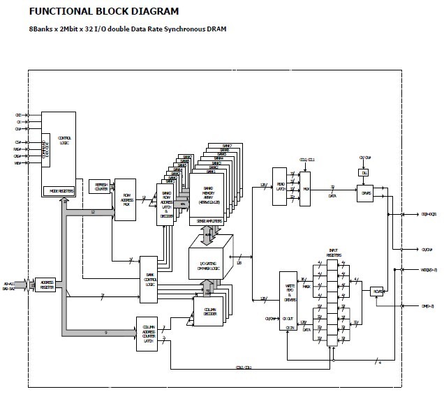
Product Summary
The Hynix H5RS5223CFR-14C is a high-speed CMOS, dynamic random-access memory containing 536,870,912 bits. The Hynix H5RS5223CFR-14C is internally configured as a eight-bank DRAM. The Hynix H5RS5223CFR-14C uses a double data rate architecture to achieve high-speed opreration. The double date rate architecture is essentially a 4n-prefetch architecture, with an interface designed to transfer two data words per clock cycle at the I/O pins. A single read or write access for the Hynix H5RS5223CFR-14C consists of a 4n-bit wide, every two-clock-cycles data transfer at the internal DRAM core and two corresponding n-bit wide, one-half-clock-cycle data transfers at the I/O pins. Read and write accesses to the Hynix H5RS5223CFR-14C is burst oriented; accesses start at a selected locations and continue for a programmed number of locations in a programmed sequence. Accesses begin with the registration of an ACTIVE command, which is then followed by a READ of WRITE command. The address bits registered coincident with the ACTIVE command are used to select the bank and row to be accessed (BA0,BA1, BA2 select the bank; A0-A11 select the row). The address bits registered coincident with the READ or WRITE command are used to select the starting column location for the burst access. Prior to normal operation, the Hynix H5RS5223CFR-14C must be initialized.
Parametrics
Absolute maximum ratings: (1)Voltage on Vdd Supply Relative to Vss: -0.5V to +2.5V; (2)Voltage on VddQ Supply Relative to Vss: -0.5V to +2.5V; (3)Voltage on Vref and Inputs Relative to Vss: -0.5V to +2.5V; (4)Voltage on I/O Pins Relative to Vss: -0.5V to VddQ +0.5V; (5)MAX Junction Temperature, TJ: +125℃; (6)Storage Temperature (plastic): -55℃ to +150℃; (7)Power Dissipation: TBD; (8)Short Circuit Output Current: 50mA.
Features
Features: (1)2.05V/ 1.8V/ 1.5V power supply supports (For more detail, Please see the Table 12 on page 43); (2)Single ended READ Strobe (RDQS) per byte; (3)Single ended WRITE Strobe (WDQS) per byte; (4)Internal, pipelined double-data-rate (DDR) architecture; two data accesses per clock cycle; (5)On Die Termination; (6)Output Driver Strength adjustment by EMRS; (7)Calibrated output driver; (8)Differential clock inputs (CK and CK); (9)Commands entered on each positive CK edge; (10)RDQS edge-aligned with data for READ; with WDQS center-aligned with data for WRITE; (11)8 internal banks for concurrent operation CAS Latency: 4 to 11 (clock); (12)Data mask (DM) for masking WRITE data; (13)4n prefetch; (14)Programmable burst lengths: 4, 8; (15)32ms, 8K-cycle auto refresh; (16)Auto precharge option; (17)Auto Refresh and Self Refresh Modes; (18)1.8V Pseudo Open Drain I/O; (19)Concurrent Auto Precharge support; (20)tRAS lockout support, Active Termination support; (21)Programmable Write latency(1, 2, 3, 4, 5, 6); (22)Boundary Scan Function with SEN pin; (23)Mirror Function with MF pin.
Diagrams